|
|
GaB Design and Consultancy Printed Circuit Board Design |
|
|
GaB Design and Consultancy Printed Circuit Board Design |
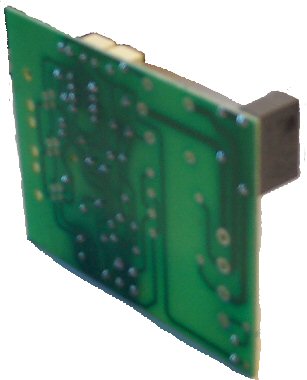 |
PCB DATA LOST !
|
|
We are able to take your existing PCB, old artworks or Gerber data and Reverse Engineer them back into our PCB package. We have successfully re-produced design files for Customers, who have lost or misplaced data, for board manufacture whilst incorporating any design changes in the process. |
|
Printed Circuit Board Design Service, PCB layout, located in Harpenden, Hertfordshire, UK, for single sided, double sided and multilayer printed circuit board designs incorporating conventional through hole components or surface mount components, SMD. Digital and analogue, analog, printed circuit board design, reversed engineering of existing artworks or printed circuit board designs using manual scanning methods, not scanfab, to recreate the printed circuit board design as a PCB design file. Schematics, net list, netlist, data and component data sheets taken with mechanical constraints to create printed circuit board, PCB, design. Check prints produced in hard copy printed format or electronic format , PDF, HPGL, DXF, AutoCad compatible for customer approval. Gerber photo tools including photoplots and N.C. Drilling data produced for printed circuit board manufacture. Files sent via E-Mail or in the post to anywhere in the UK, England. Small firm based in Harpenden, Hertfordshire, Herts. servicing surrounding bedfordshire, beds, buckinghamshire, buck, surrey, london.