|
|
GaB Design and Consultancy Printed Circuit Board Design |
|
|
GaB Design and Consultancy Printed Circuit Board Design |
|
|
|||
We aim to be as competitive as possible with our pricing and offer a low minimum charge of £60-00 for the less complex designs and any minor modifications to existing designs.
|
|||
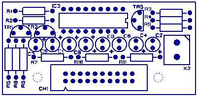
Typical Design charged at the minimum rate.£75-00 |
|
||
|
|
Includes PCB Design, Electronic check prints (eg. PDF format) for approval and full set of Photo tools (Gerber and N.C. Drilling data files only) for board manufacture. | ||
P
Printed Circuit Board Design Service, PCB layout, located in Harpenden, Hertfordshire, UK, for single sided, double sided and multilayer printed circuit board designs incorporating conventional through hole components or surface mount components, SMD. Digital and analogue, analog, printed circuit board design, reversed engineering of existing artworks or printed circuit board designs using manual scanning methods, not scanfab, to recreate the printed circuit board design as a PCB design file. Schematics, net list, netlist, data and component data sheets taken with mechanical constraints to create printed circuit board, PCB, design. Check prints produced in hard copy printed format or electronic format , PDF, HPGL, DXF, AutoCad compatible for customer approval. Gerber photo tools including photoplots and N.C. Drilling data produced for printed circuit board manufacture. Files sent via E-Mail or in the post to anywhere in the UK, England. Small firm based in Harpenden, Hertfordshire, Herts. servicing surrounding bedfordshire, beds, buckinghamshire, buck, surrey, london.